Original research contributions
Impact ionisation and light emission
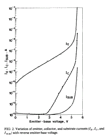
In the mid 1980s volatile memories had been observed to degrade when in close proximity to MOSFET's operating in weak avalanche. At that time it was believed that the memories were discharged by excess minority carriers produced by a process of secondary impact ionisation in the region of the transistors. While working at Liverpool University we proposed that light emitted from a MOSFET during weak avalanche and subsequently reabsorbed created the minority carriers in the substrate1. We confirmed this process by observing the current generated in the substrate of a bipolar transistor during emitter-base avalanche due to light emission light emission. Direct evidence of light emission from MOSFETs was provided in later work.2 Interestingly, a process of impact ionisation in the neutral region of the base of a BJT transistor 3 and related to secondary impact ionisation was observed as a collective current. Surprisingly, there were no previous reports of a bipolar transistor operated in this mode.
Above supply voltage energy distribution
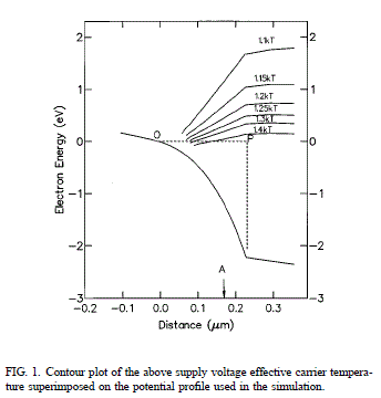
As supply voltages to MOSFETs continued to be scaled in the 1990s hot carrier effects were more related to the energy supplied to the charge carriers in the channel than the electric field near the drain. Monte Carlo simulations reported in the literature suggested that the distribution of charge carriers in the region of energy above that provided by the drain voltage has the form of a Boltzmann distribution with an effective temperature equal to that of the lattice, TL. However, the density of charge carriers in this region is very low and the Monte Carlo data was relatively noisy. At Birmingham University we developed a semi-analytic technique for obtaining the energy distribution function in regions of low probability4. Results based on this model showed the effective temperature of the energy distribution to be above TL, only approaching the lattice temperature asymptotically.5A detailed physical explanation of this phenomenon and other effects were described in a later paper.6
Electron-electron interactions
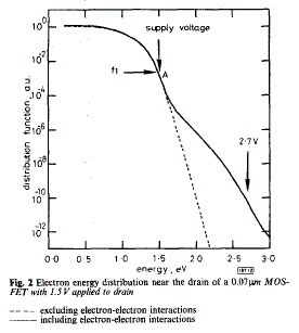
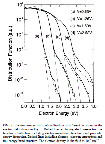
Even when the drain voltage applied to MOSFETs was scaled below 3V current was still observed to flow in the gate of the device. This was unexpected as even charge carriers travelling ballistically to the drain would not have sufficient energy to overcome the potential barrier to the oxide. One possible mechanism for this was energy gain through electron-electron collisions near the drain on MOSFET. However, the inclusion of these scattering events in Monte Carlo simulations was difficult particularly for low probability events. The simulations we were undertaking at Birmingham had the advantage that they were based on an iterative technique into which electron-electron collisions could be more readily integrated. We showed that a hot carrier distribution was significantly by these interactions.7,8,9
X-ray propagation in carbon nanotubes
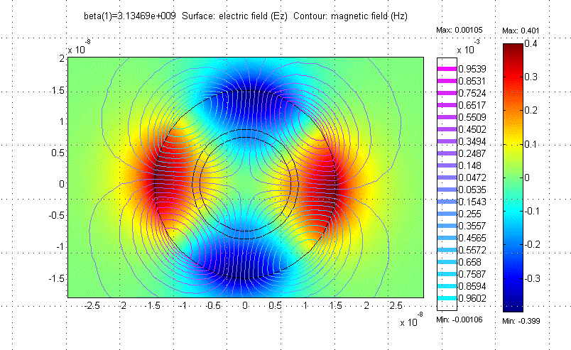
With the fabrication of devices having physical dimensions of the order of nanometres in the 2000s it was desirable to develop new techniques for patterning and characterisation. A novel method that we explored in conjunction with Anthony O'Neill at Newcastle University was the exploitation x-ray propagation in carbon nanotubes. An early analysis had shown that the wall of a carbon nanotube was too thin to confine x-rays within the nanotube. However, our simulations showed that suitably coated carbon nanotubes could sustain x-ray modes and therefore have potential use for patterning and analysis.10
Conductance of graphene nonoribbons and carbon nanotubes
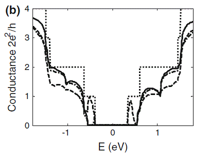
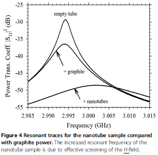
Carbon-based electronics is of interest because of the potential for ballistic challenge transport within devices. Graphene is attractive as it is planar and compatible with silicon and established patterning techniques where is carbon nanotubes are free from edge effects. In modelling charge transport in graphene nanoribbons we observed that the accuracy of the simulation was significantly improved with the inclusion of third nearest neighbour interactions.11 Our microwave studies undertaken in conjunction with Prof. Adrian Porch at Cardiff University have shown that some carbon nanotube powders suggest that enormous sheet conductivities.12
[1] Alternative Mechanism for Substrate Minority-Carrier Injection in MOS Devices Operating in Low-Level Avalanche
P A Childs, W Eccleston and R A Stuart, Electronics Letters 17(8), 281 (1981)
DOI: 10.1049/el:19810197[2] EVIDENCE OF OPTICAL-GENERATION OF MINORITY-CARRIERS FROM SATURATED MOS-TRANSISTORS
P A Childs, R A Stuart and W Eccleston, SOLID-STATE ELECTRONICS 26(7), 162 (1983)
DOI: 10.1016/0038-1101(83)90025-4[3] Impact Ionization Induced Minority-Carrier Injection by Avalanching p-n Junctions
P A Childs and W Eccleston, JOURNAL OF APPLIED PHYSICS 55(12), 4304 (1984)
DOI: 10.1063/1.333041[4] Spatially Transient Hot-Electron Distributions in Silicon Determined from the Chambers Path-Integral Solution of the Boltzmann Transport-Equation
C C C Leung and P A Childs, Solid State Electronics 36(7), 1001 (1993)
DOI: 10.1016/0038-1101(93)90117-9[5] On the above supply voltage hot carrier distribution in semiconductor devices
P A Childs and C C C Leung, APPLIED PHYSICS LETTERS 66(2), 162 (1995)
DOI: 10.1063/1.113550[6] Hot carrier quasi-ballistic transport in semiconductor devices
P A Childs and D W dyke, SOLID-STATE ELECTRONICS 48(5), 765 (2004)
DOI: 10.1016/j.sse.2003.12.008[7] New Mechanism of Hot-Carrier Generation in very Short-Channel MOSFETs
C C C Leung and P A Childs, Electronics Letters 31(2), 139 (1995)
DOI: 10.1049/el:19950091[8] One-dimensional solution of the Boltzmann transport equation including electron-electron interactions
P A Childs and C C C Leung, JOURNAL OF APPLIED PHYSICS 79(1), 222 (1996)
DOI: 10.1063/1.360935[9] High-energy electron-electron interactions in silicon and their effect on hot carrier energy distributions
M Y Chang, D W Dyke, C C C Leung and P A Childs, JOURNAL OF APPLIED PHYSICS 82(6), 2974 (1997)
DOI: 10.1063/1.366133[10] Propagation of X-rays in carbon nanotubes in semiconductors
P A Childs and A G O'Neill, PHYSICA E-LOW-DIMENSIONAL SYSTEMS and NANOSTRUCTURES 19(1-2), 153 (2003)
DOI: 10.1016/S1386-9477(03)00311-4[11] Conductance of Graphene Nanoribbon Junctions and the Tight Binding Model
Y Wu and P A Childs, NANOSCALE RESEARCH LETTERS 6, Article Number: 62 (2011)
DOI: 10.1007/s11671-010-9791-y[12] Microwave characterisation of carbon nanotube powders
A Porch, D I Odili and P A Childs, NANOSCALE RESEARCH LETTERS 7, Article Number: 429 (2012)
DOI: 10.1186/1556-276X-7-429